Per- and polyfluoroalkyl substances (PFAS), are a group of man-made ‘forever chemicals’ widely used since the 1940s in products such as non-stick cookware, cosmetics, and food packaging due to their resistance to grease, water, heat, and oil.
Their strong chemical bonds make them extremely persistent, with 97% of the U.S. population having PFAS in their blood. PFAS have been linked to multiple health issues, including cancer, immune system disruption, thyroid disease, and liver and kidney damage.
Semiconductors, or microchips, are essential components in electronics like cell phones, computers, and medical diagnostic equipment (SIA).
The semiconductor industry, a leader in global R&D and manufacturing, has long relied on high-performance per-and polyfluoroalkyl substances (PFAS) additives, particularly in antireflective and photoresist coatings, for advanced chip production.
In 2024, the U.S. Environmental Protection Agency (EPA) established the first national, legally enforceable drinking water standards for PFAS to protect communities from exposure. The EPA set Maximum Contaminant Levels (MCLs) at 4 parts per trillion for PFOA and PFOS, and 10 parts per trillion for PFNA, PFHxS, and GenX chemicals. PFOA and PFOS have also been classified as hazardous substances under CERCLA.
Emerging PFAS regulations have led many semiconductor fabrication companies to proactively seek PFAS destruction solutions, driven by the future liability associated with PFAS-contaminated effluent wastewater. Semiconductor manufacturers have also explored PFAS alternatives with little success, instead turning to short-chain (4 carbon atoms or fewer) PFAS compounds which pose similar toxicological risks based on recent studies.
As the regulatory framework for PFAS becomes more stringent, it is increasingly important for fabrication producers to explore PFAS treatment solutions that are available now.
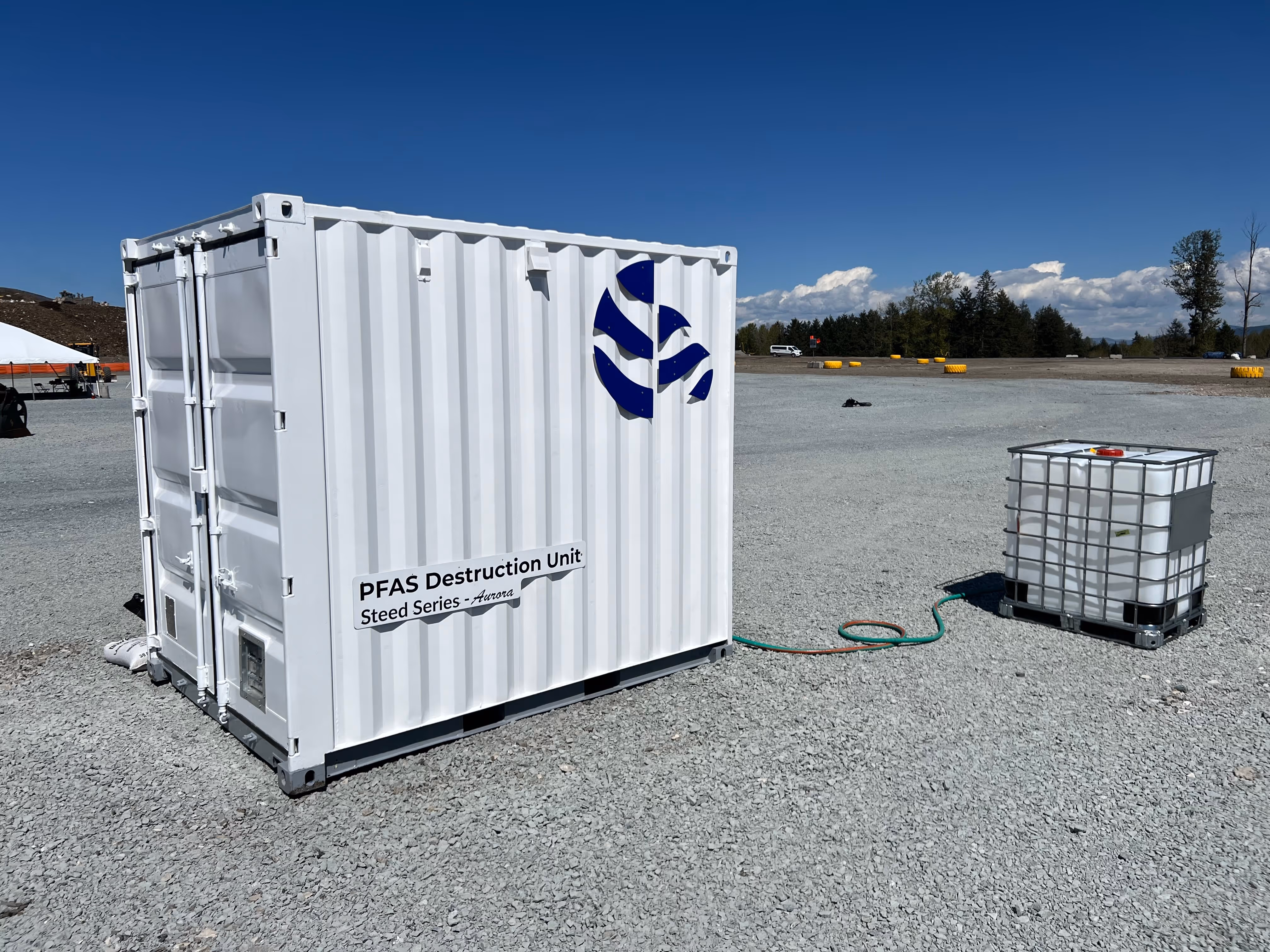
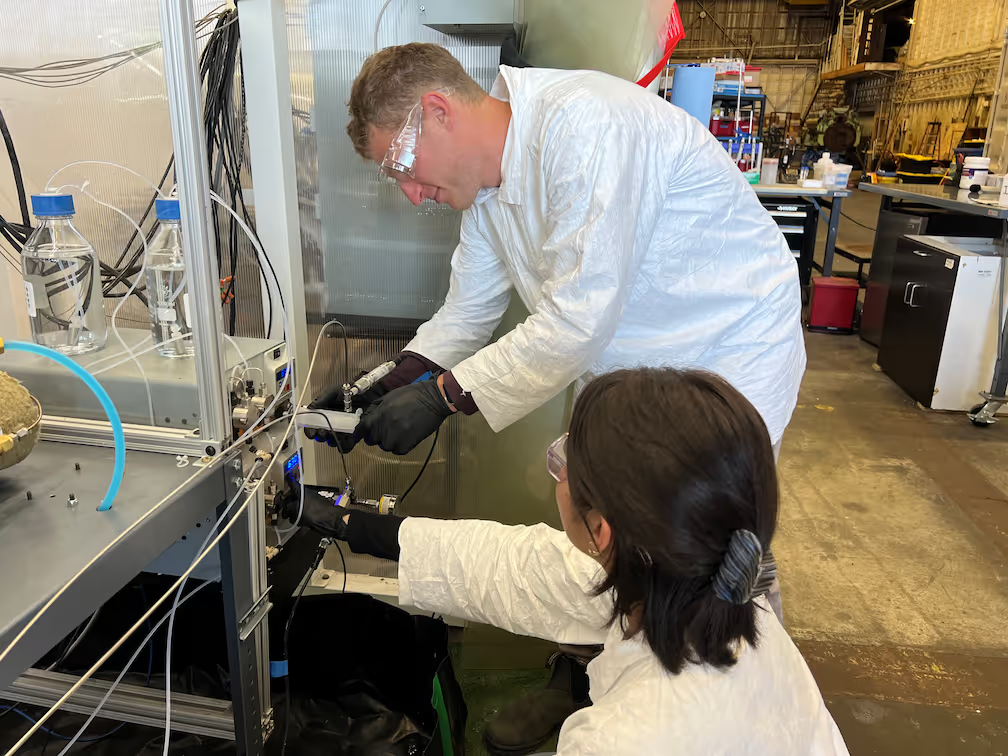
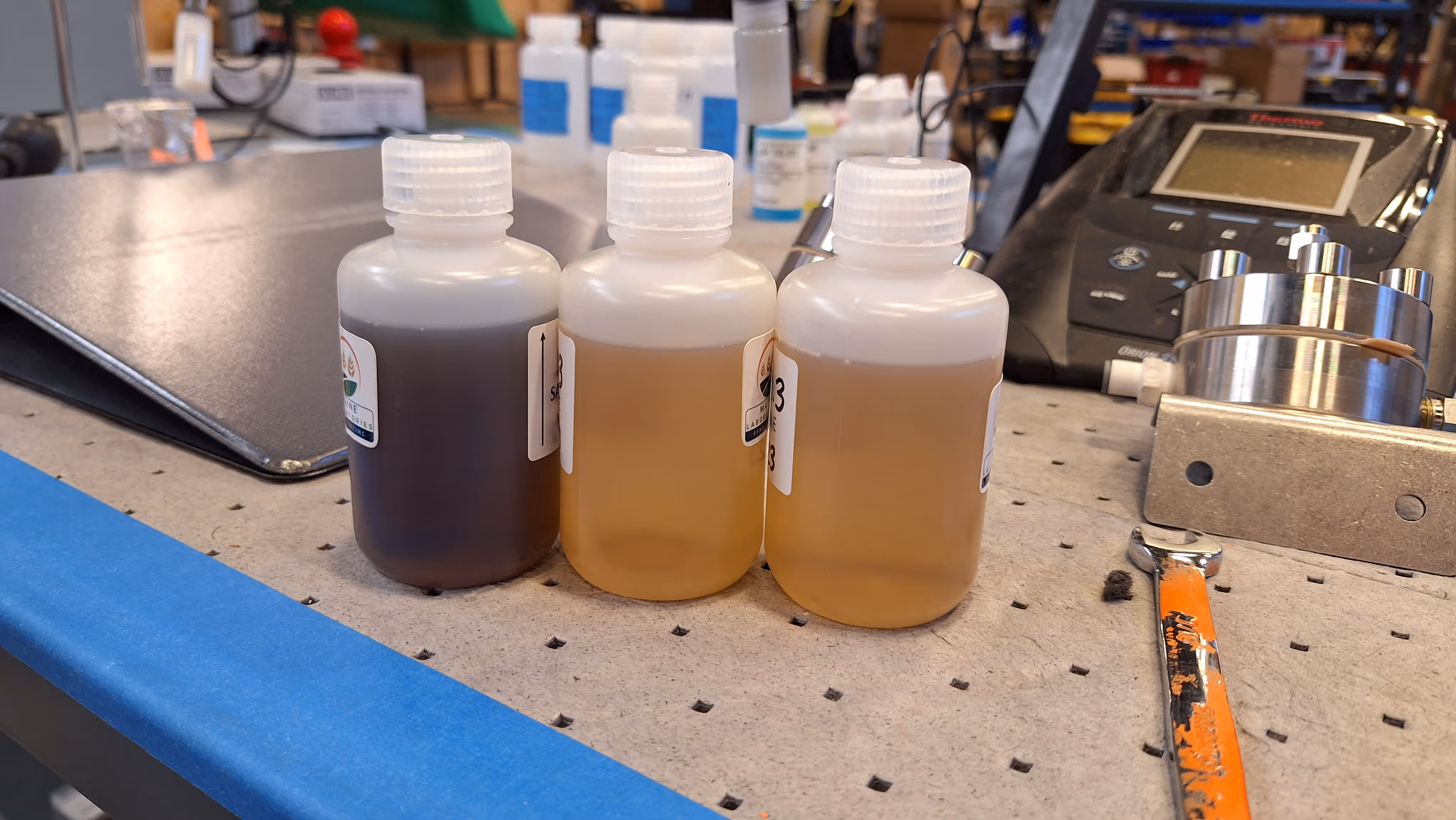
Aquagga’s HALT technology combines temperature, pressure, and an alkaline amendment to effectively break the strong carbon-fluorine bonds that hold PFAS together, achieving complete mineralization.
.gif)
Front end production involves wafer fabrication, using processes like photolithography and etching to create circuit patterns on silicon wafers. These processes generate wastewater and byproducts that contain PFAS.
Back end production focuses on assembling and packaging semiconductor chips. Additional waste streams are created, including those that may contain PFAS from packaging (moldings and mountings) and testing materials.

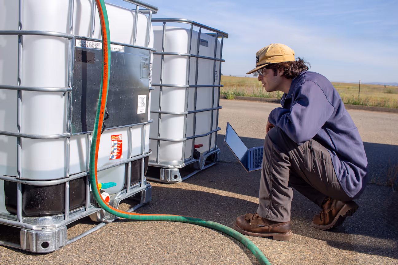
When treating PFAS, the recommended approach involves separation, concentration, and destruction. Aquagga’s HALT technology interfaces with separation and concentration technologies such as reverse osmosis (RO), regenerable ion-exchange resin (IXR), and foam fractionation to treat high-concentration secondary waste streams.
As a final step in the PFAS treatment process, the HALT system then intakes this PFAS-rich feedstock for complete destruction, resulting in clean water without any unwanted byproducts. HALT can be integrated for both front and back end fabrication.
HALT Value-Adds


Aquagga is a team of PFAS specialists dedicated to one of the most persistent and challenging pollutants of the 21st century. Committed to advancing the PFAS sector, Aquagga engages in cutting-edge research to develop new methods for detecting and destroying contaminants that affect global water resources.


